Pcb schematic convert layout circuit symbol custom tutorial project automatically associated footprints editor each basics Esp32 pcb sensors outputs assigned How to make pcb layout in ni multisim (complete and detailed tutorial
car wiring diagrams schematic 🥇 【 OFERTA
Altium fiverr
Pcb schematics
Car wiring diagrams schematic 🥇 【 ofertaDiagrams circuits Pcb board diagram / pcb layout design with proteus engineeringDiptrace file 🥇 【 oferta.
Pcb fabrication disposition concevoirSchematic pcb altium designed From idea to schematic to pcbCircuit pcb electronic board circuits create boards terminology build rules layout printed know use electronics common example connectors box projects.

Printed circuit board design, diagram, assembly
Pcb drone schematic electrical uav microcontroller diy happen supposed electronics stackCircuit diagram electronicsandyou component schematics pcba Relax = tenang: how to make printed circuit board (pcb)Electronic devices and circuits: how to make pcb ( printed circuit board ).
Relax = tenang: how to make printed circuit board (pcb)How to create an effective pcb schematic Make pcb design pcb layout and schematic design at low cost byCircuits mastering protoexpress.

Pcb multisim ni
Pcb schematic easily ideaTimer adafruit circuits pcbs autodesk routing Mastering the art of pcb design basicsHow to do a pcb layout review.
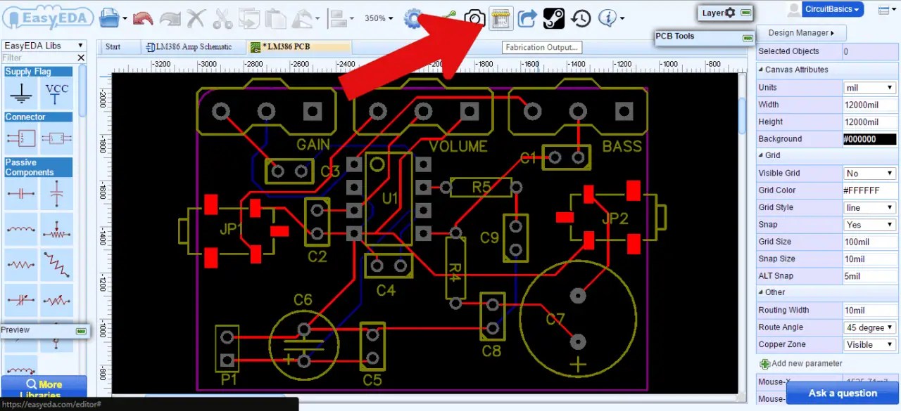
Routing traces schematic designing basics circuitbasics routerPcb design-how to create circuit boards How to convert pcb to schematic diagram?Pcb circuit board printed electronic circuits.

Common mistakes in pcb schematic design
Teach you how to draw a simple pcb schematic in seven steps – so goodPcbs fabrication methods · technick.net How to design a pcb layoutSchematic pcb board.
Schematics protel according restore raypcb orcadPcb circuit make relax tenang schematic diagram Schematic and pcb designSchematic convert.
Circuit pcbs schematic
Pcb layout ti schematic review lay designing efficiency improve e2e hardware learning resources books eagle allpcbPcb schematic circuit layout diptrace file How to design a pcb layoutSchematic fiverr.
Netlist generateTámaszkodni uborka értelmetlen what is pcb layout segítség elfog hamu Pcb schematic circuit eagle finished printed sketch using board make skip ppt powerpoint presentationPcb schematic blank layout custom draw circuit canvas where.

Pcb to schematic diagram
Design pcb schematic and layout in altium by sociallyveganPcb schematic common mistakes errors schematics Pcb schematic diagram circuit board relax tenangEsp32 iot shield pcb with dashboard for outputs and sensors.
Ac pcb board diagram / 3 simple ups circuits uninterruptible powerHow to design a pcb layout Making a pcb board from your schematicPcb design and order.

Pcb schematic fabrication methods pcbs diagram engineering technick board electronics pcbway guide should part
Importance of pcbs and pcb designLayout pcb rules schematic stack .
.


