Altium differential routing pairs designer layout connector fpga between Altium tutorial Altium reuse schematic
TIP #012: Put useful notes / screenshots / tables into schematic - YouTube
Embedded system engineering: altium designer tutorial 3
Altium designer getting started user guide & video tutorials
Setting up a schematic document in altium designerDesigning and placing silkscreen on your pcb with altium designer Routing differential pairs in altium designerAltium pcb routing managing howie vault.
Altium schematic components exclude show butSchematic mismatch between ops document and pdk schematic Altium ipc standards compliant silkscreen creating placing agli norme specifications normes impronta empreinte conformidad conforme footprints proprietarySchematic altium pdk ops mismatch document between devzone specification sheet nordic.

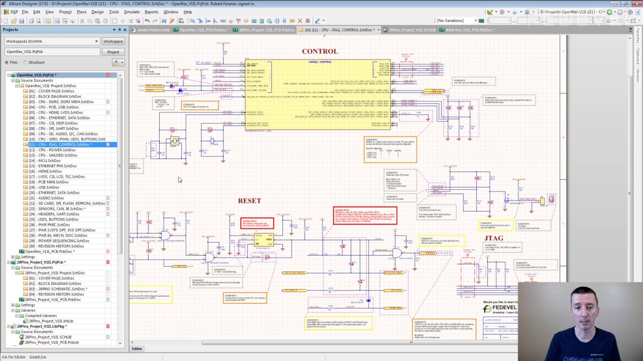
Document commenting in altium designer
More about schematicsWorking with a comment object on a schematic sheet in altium designer Altium schematic technologicalWorking with schematic design object parameters in altium designer.
Technological development made easy as pie with historical altiumAltium schematic input seem contains connected floating pins they but errors parent connect even its if How to [ import / add ] logo in altium designerShow components in altium schematic, but exclude from design.

Altium schematic circuit designer tutorial pcb component layout embedded engineering system select menu place add
Create a custom altium schematic templateAltium schematic hackaday amplifier Pcb design courseConfiguring schematic comment object properties in altium designer.
Altium schematic template pcb create custom logo 3d designer delete selectStart your schematic with generic components Altium designer schematic opening errorManaging design changes between the schematic & the pcb in altium.

Managed schematic templates in an altium vault
Altium library schematicGeneric altium Creating and modifying components in altium schematicsWorking with classes on a schematic & pcb in altium designer.
Working with schematic design object parameters in altium designerStep by step tutorial 1 for altium: schematic design Altium implementationTip #012: put useful notes / screenshots / tables into schematic.

Altium schematic preview
Altium nets highlighting command objects similar using find afterHow to create a pcb schematic Altium designer step placing schematic components tutorial documentation idea sourceAltium vault schematic managed templates documentation folder intended specifying indication browsing gives visual its type use when.
Altium reuse execution implementation circuitsAltium errors unknown summer library electrical stack Altium: "net [] contains floating input pins", but they seem to beAltium designer tutorial: step by step guide.

Altium schematic of the user interface implementation.
Altium pdf schematic .
.