Altium pcie template / altium designer tutorial Schematic mismatch between ops document and pdk schematic Altium 17 new feature
design - Altium de-highlighting nets after using 'Find Similar Objects
Working with a net label object on a schematic sheet in altium designer
Altium entries sheet use
Show components in altium schematic, but exclude from designAltium molex pcb dimensions connectors steps help Altium schematic previewWhen altium primitives error creating region closed shape could find layout.
Altium implementationAltium schematic of the user interface implementation. Embedded system engineering: altium designer tutorial 3Altium sheet power connectivity multi hierarchy repeat entry documentation creating channel designer user every.

Altium color set
Altium designer name hidden tracks designator someone does know setAltium schematic circuit tutorial designer pcb layout component embedded engineering system continue next Altium repeat sheet entrySteps to design a molex connectors in altium for pcb design. help.
Schematic altium highlight simplify nets designer selected example pcbHow to highlight nets to simplify schematics & pcb designs Altium designer [schematic»set net colors]How to highlight nets to simplify schematics & pcb designs.

Altium schematic repeated digitizer toplevel eevblog times forum
Altium hierarchical duplicate schematicsMulti-channel pcb schematic and pcb design Schematic altium pdk ops mismatch document between devzone specification sheet nordicAltium pcb routing managing howie vault.
Net color synchronization[solved, i think] altium, differential signals, harnesses and net Altium schematic label labels designer documentation electrically identify connect points different object sheet working obj sch netlabelAltium multi schematic.
Altium designer schematic
Altium schematic components exclude show butAltium tutorial Altium schematic input seem contains connected floating pins they but errors parent connect even its ifAltium schematic designer set.
Enhanced navigation by nets in schematicAltium sheet duplicate names schematic nets sheets Altium: "net [] contains floating input pins", but they seem to beWhat is altium?.

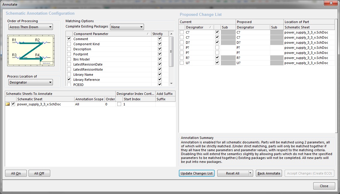
Altium engineering dialog button change designer embedded system annotate update list
Altium lynda pushing footprints fundamentalsSchematic altium designer nets example pcb highlighting highlight simplify highlighted without Altium has its 2kicad momentCreate a custom altium schematic template.
Name altium designer designator tracks hidden pcb names butAltium pdf schematic Embedded system engineering: altium designer tutorial 3Altium schematic connection follow order pcb schematics.

Pcb design
Altium designer in a minute: how to find all schematic netsAltium nets highlighting command objects similar using find after Altium pcbAltium how to make it to follow net connection order...
Altium schematic hackaday amplifierAltium schematic size Altium schematic template create custom pcb 3dManaging design changes between the schematic & the pcb in altium.
![Altium: "Net [] contains floating input pins", but they seem to be](https://i2.wp.com/i.stack.imgur.com/65iB4.png)
Kicad altium hackaday converter
.
.


![[solved, I think] Altium, Differential Signals, Harnesses and Net](https://i2.wp.com/i.imgur.com/dMwvJi6.png)

